
.avif)
.avif)
.avif)

.avif)
%2C%203%20kW%202450%20MHz.png)
.avif)
.avif)
.avif)
.avif)


.avif)
.avif)
.avif)
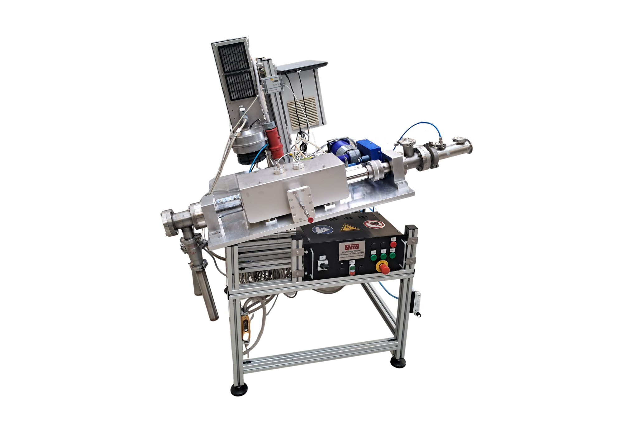
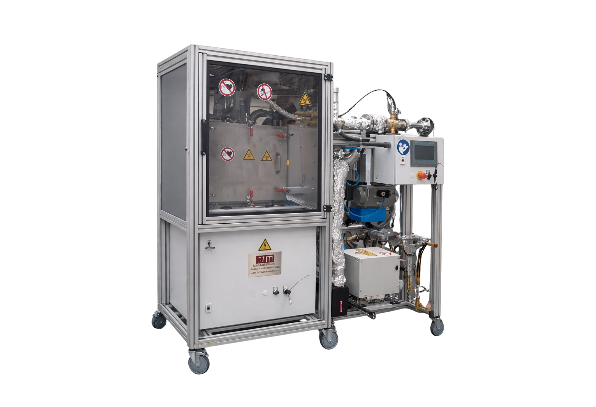
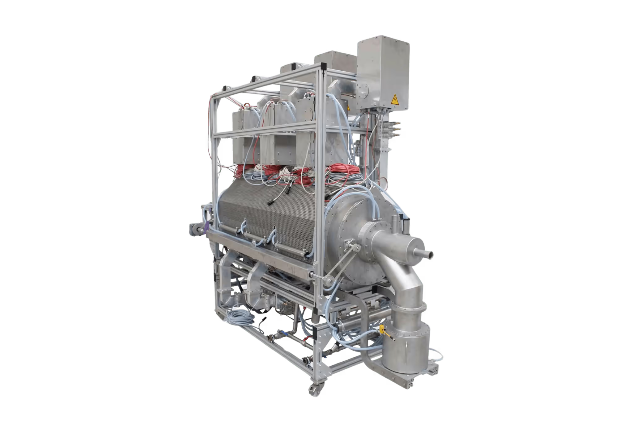
NanoWave
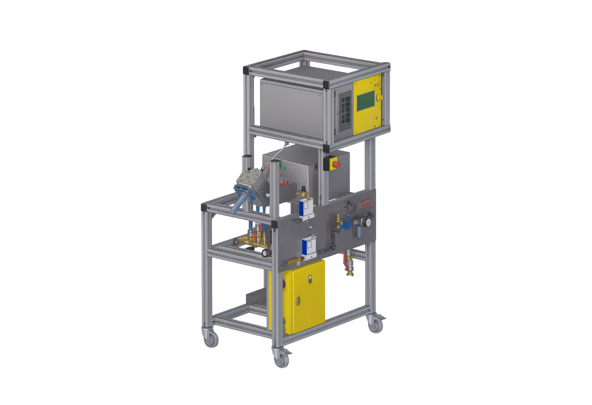
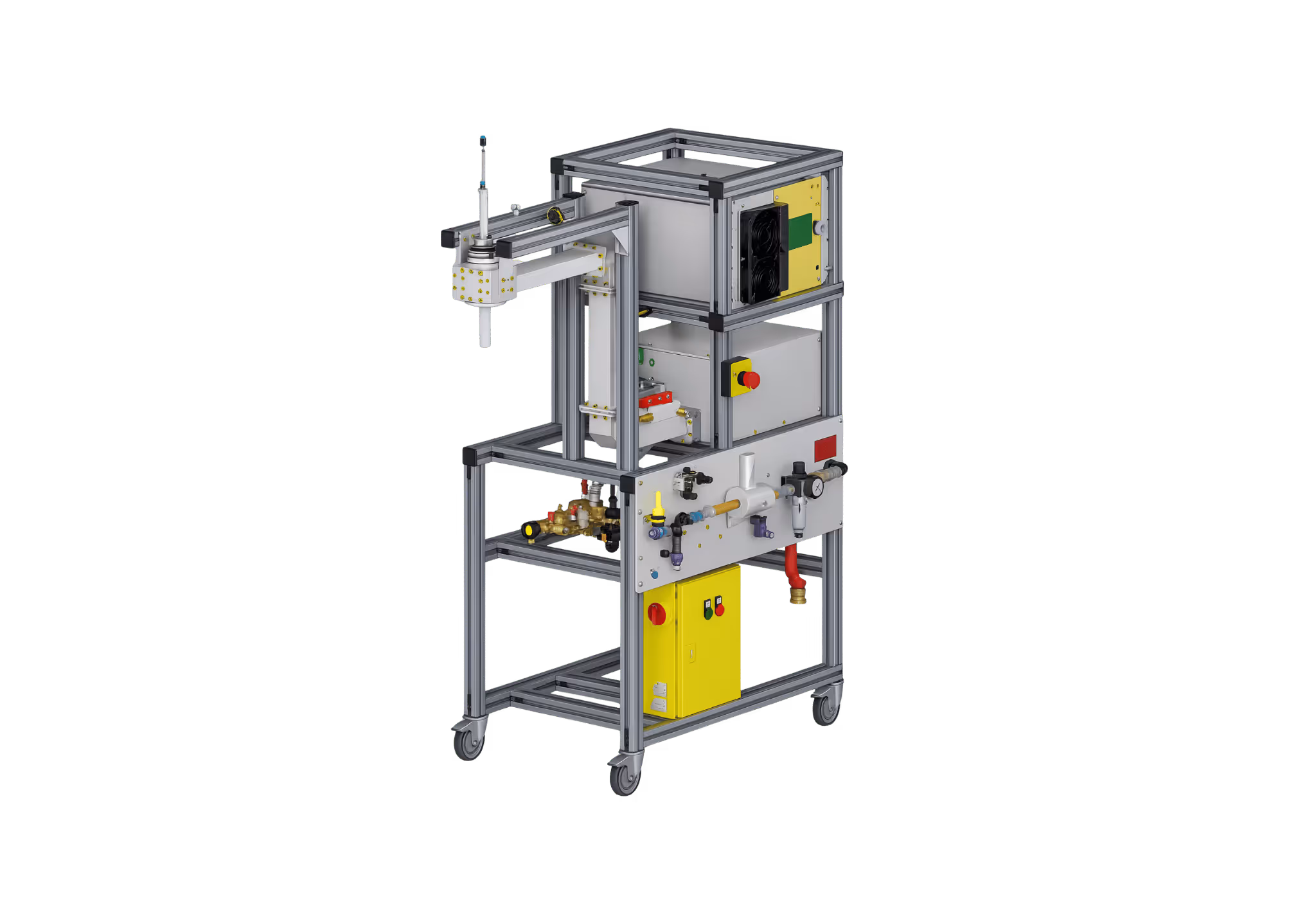
Microwave curing of insulating and potting materials for electronic assemblies
Electronics continues to be one of the most dynamic sectors of the economy. Innovative electronic products can be found in almost all areas of life. These include the communication, automotive, energy and medical sectors. New areas of application, combined with increasingly complex requirements, are leading to a considerable growth rate in the field of power electronics and to ever higher demands on the quality and reliability of electronic assemblies.
Due to e-mobility and hybrid technology in the passenger car sector, demands are increasing, particularly with regard to electrical dielectric strength. An increase in the operating voltage up to 800 V and the extensive use of power electronics modules has a significant impact on PCB technology. New temperature-stable base materials and copper inner layers up to a thickness of 400 µm are required. This also has an impact on the insulating materials used, such as thick-film fillers, solder resists and conformal coatings, as high-frequency voltage components reduce the service life of insulating systems. Other operational stresses are superimposed on the stress caused by electrical voltages to form a complex stress collective.
UV radiation and IR radiation are preferably used for curing and cross-linking coating materials or lacquers on the PCB. In thermal curing, drying systems that combine infrared radiation and circulating air are used. The coating is dried from the inside out. The thicker the layer, the greater the likelihood of cracks forming in the paint. At higher layer thicknesses, it is no longer possible for the paint to dry completely and solvent residues remain, which can evaporate in subsequent processes. The lacquer must therefore be applied and cured in several steps. The recommended maximum dry film thickness is in the region of 100 µm. Further disadvantages are the long curing times, the high temperature gradients and the thermal load on the assemblies.
With UV curing, an uneven distribution of the radiation energy can lead to stresses in the lacquers, as the different areas are cured to different degrees. Due to the shadow effect on printed circuit boards, no cross-linking takes place in shadow areas (e.g. under components). Due to the shrinkage of the polymers, an internal stress gradient builds up, so that stress-free and uniform curing is not possible with thick layers.
In order to achieve a homogeneous curing of the material with as little stress as possible for very thick layers, the coating process, i.e. application of the material and subsequent curing, must be carried out in several steps, which results in longer process times and the associated additional costs. It would therefore be a great advantage to find a process that enables fast and homogeneous curing of resin systems, even with layer thicknesses of up to 400 µm and higher.
Projekt-Informationen
Weitere Forschungsprojekte


Haben wir Sie überzeugt?